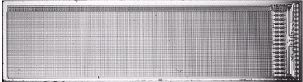
Fingerprint sensors
Here are the fingerprint sensors that have at least existed once, excepted (simple) optical sensors.
I know, this is a very very long page, because there are many tentatives and products, and I decidedto get all of them in one page -because having a hundred pages to manually manage would be tedious!
So I propose as a start just a list where you can click to go to the manufacturer you want to see.Another solution is to use the "find in the page" of your brother, or use google.
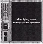
Silicon manufacturers are fabricating these sensors.
List of compagnies
Pionners
Here are some links related to pionner stories about making solid-state fingerprint sensors.
Opsis
- (1994 Jul) Opsis SA offered a device using a conductive membrane deposited on a CMOS chip.
I'm still wondering if it is related to the Teruhiko Tamori R&D... - For the records, a (simplified) local copy of the Opsis website years ago !
Thomson-CSF > 2000 > Atmel
Philips
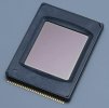
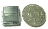
Harris >> Authentec > 2012 > Apple
- (1998 Dec) Authentec spin-off from Harris. Bought Atrua in 2009, merged with Upek in 2010. Bought by Apple in July 2012. Production no more available as of May 2013. Manufacturer: TSMC, packaging: Signetics. RF modulation sensing fingerprint sensor.
- White paper.
- 92x8 pixels @500dpi
- (2010 Nov) AES850 (with navigation)
- Apple era
- (2013) TMDR92 (or ME296). 88x88 pixels @ 508 dpi. See also the Apple page.
- (2015 Sep) a new sensor chip + NVT8417 companion chip (dated 2014).
The resolution seems to be still 508 dpi, but looks like it is not a square chip: 112x96 pixels (I am unsure if I'm still able to properly count pixels, that's weird numbers...), so a little bit better than the previous version.
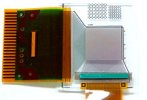
STm > 2004 > Upek > 2010 > Authentec
- Upek spin-off from ST Microelectronics in 2004. Merged with Authentec in 2010, which has been bought by Apple in 2012. Note that some Upek products are now available through Digital Persona, now CrossMatch.
- Upek flyer (2009).
- TouchChip TCS1 family 360x256 pixels @508dpi
- (2001) TouchChip TCS1AD: TCS1AD flyer.
- (2002 Oct) TouchChip TCS1CD (gold coating, FIPS-201 PIV certified)
- () TouchChip TCS1ST (SteelCoat)
- Still available at CrossMatch (checked 2016 Feb). TCS1 flyer.
- TouchChip TCS2 family 288x208 pixels @508dpi
- (2001) TouchChip TCS2AF 288x208 pixels @508dpi TCS2AF flyer.
- (2002 Oct) TouchChip TCS2CF 288x208 pixels @508dpi
- () TouchChip TCS2S (SteelCoat)
- Still available at CrossMatch (checked 2016 Feb). TCS2 flyer.
- TCS3 family 248x4 pixels @508dpi
- (2003 Nov) TouchStrip TCS3B TCS3B flyer.
- TouchStrip TCS4 family 192x4 pixels @508dpi
- (2006 Feb) TouchStrip TCS4
- () TouchStrip TCS4A, TCS4B, TCS4C, TCS4E
- TouchStrip TCS5 family 144x4 pixels @508dpi
- (2008 Jun) TouchStrip TCS5
- (2009 Sep) TouchStrip TCS5C SteelCoat
- (2011 Mar) TouchStrip TCS5D
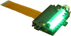
- (2009 Jun) The TCS5 + LED = TouchLight
Lucent > Veridicom
- (1997 May) Veridicom spin-off from Lucent (lucent.com is not working anymore, if you want know why : What Happened to Lucent.com?) develops a capacitive fingerprint sensor
- (1998 Feb) A robust, 1.8 V 250 /spl mu/W direct-contact 500 dpi fingerprint sensor Inglis, C.; Manchanda, L. ; Comizzoll, R. ; Dickinson, A. ; Martin, E. ; Mandis, S. ; Silveman, P. ; Weber, G. ; Ackland, B. ; O'Gorman, L.
- (1998) FPS100 datasheet
- (2000) FPS110 datasheet
- (2000 Jul) 5thsense FPS200 (same sensor as Fujitsu) flyer datasheet
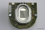
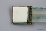
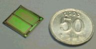
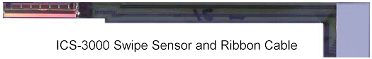
- (2001 Dec) publication of a paper describing a swipe sensor: Innovations in fingerprint capture devices Xiongwu Xia., Lawrence O'Gorman.
- Veridicom history: Fingerprint of failure / Bill Roberts 2002
- See Fujitsu and the MBF family.
Michigan University
CEA-Leti
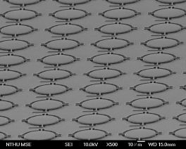
- (2014) PiezoMat proposes a new technology of high-resolution fingerprint sensors based on a matrix of interconnected piezoelectric nanowires
Fingerprint Cards
- Fingerprint Cards is proposing RF modulation fingerprint sensors.
- Foundry: SMIC, packaging: Amkor.
- Partnership with Shenzhen O-Film Tech.
- In 2012, Apple buys Authentec+Upek and stops the production. Validity has not yet a real offer, and Atmel stopped in 2008. Smartphone makers are becoming orphan, without fingerprint sensor providers: what a piece of luck! Fingerprint Cards took the opportunity...
- Some specific partnerships with CrucialTec and Q-Tech, and the situation is not so clear. See further.
- (1997) FPC1000 originally developped with Xensor. For the records: local copy of the old webpage.
- (2010 Dec) FPC1080A : 128x8 pixels @508dpi (note the change of resolution) FPC1080A flyer
- (2012) Authentec disappears... and (2013) Apple launches the iPhone 5S
- (2013 Nov) the FPC1020 is announced. 192x192 pixels @508dpi FPC1020 flyer
- (2014 Apr) the FPC1021 is announced, 30% smaller. 160x160 pixels @508dpi FPC1021 flyer
- (2014 Nov) FPC1025 complements FPC1021. FPC1025 flyer
- (2015 May) Two new touch fingerprint sensors, FPC1022 and FPC1035. 112x88 pixels.
- FPC1022 flyer
- FPC1035 flyer
- Have a look at the FPC2050 : likely a companion chip.
- (2015 Sep) FPC introduces the FPC OneTouch® FPC1200 series of touch fingerprint sensors. The new sensors can be mounted under a sheet of glass or ceramics. In fact, only zirconia at the moment, likely thanks to its huge relative dielectric permittivity...
Two devices: a small FPC1245 and a large FPC1225. - FPC1200 series flyer
- (2016 Mar) Reverse engineering from Sitri of the Xiaomi Mi5: FPC1245, with O-Film
192x56 pixels @508 dpi
- (2016 Feb) MWC 2016. We can see in the box a FPC1320 which has never been announced.
- (2016 Feb) Precise Biometrics signs license agreement with Fingerprint Cards for smart cards.
- (2016 Feb) Fingerprint Cards (FPC) launches FPC1268, a new touch fingerprint sensor in the FPC1200 series with FPC OneTouch®. The new sensor can be mounted under the cover glass of the smartphone. The first release of FPC1268 will enable cover glass of 300 µm, however the sensor technology used in FPC1268 extends to enable cover glass of up to 400 µm. Teamed with TPK.
- (2016 Feb) Fingerprint Cards extends security for fingerprint sensors, by introducing FPCLiveTouch. "Increases the security by being able to detect spoofs". No technical info given. Guess a pure software method?
- (2016 Apr) LG Innotek unveiles innovative fingerprint sensor module without button. LG Innotek cut a shallow furrow of 0.01inches (0.3mm) thick on the lower backside of the cover glass and installed the fingerprint sensor inside of it. Fingerprint Cards sensor.
- (2016 Jun) The FPC1028 is unveiled.
"smallest to date" ?x? pixels @? dpi - (2017 Sep) Huawei Maimang 6 : first launch.
- (2016 Oct) The FPC1235 for Ceramics in the Xiaomi Mix (first launch).
- (2017) The FPC1075 touch sensor size between FPC1035 and FPC1025.
- (2017 Oct) first FPC1075 on the market.
(2017) 3 types of sensors & 3 types of placement: front, rear, side:
- Spray coating: FPC1025, FPC1028, FPC1035, FPC1075, FPC1145, FPC1155
- Ceramics: FPC1245, FPC1235
- Glass: FPC1268
Brochure 2017 smartphones tablets
- (2017 Nov) Fingerprint Cards explains in their Technology Update why ultrasonic sensing is better for a full in-display fingerprint sensor. (local copy).
Looks to work more or less like the Optel sensor.
(2018 Feb)
- Spray coating: FPC1025, FPC1028, FPC1035, FPC1075, FPC1145, FPC1155
- Ceramics: FPC1235, FPC1245, FPC1235, FPC1247-Z, FPC1263, FPC1291-Z
- Glass: FPC1228, FPC1247-G, FPC1262, FPC1265, FPC1266, FPC1267, FPC1268, FPC1272, FPC1291-G
- (2018 Feb) Fingerprint Cards launches FPC1291, the first commercial third-generation fingerprint sensor.
- (2018 Jun) Fingerprint Cards AB launches fourth-generation fingerprint sensor: FPC1511, next generation fingerprint sensor for Smartphones. Full qualification of FPC1511 is scheduled for the third quarter of 2018, and the first commercial smartphones integrating FPC1511 are expected to be launched in late 2018 or early 2019.
- (2019 Feb) Fingerprint Cards launches FPC1610, its first optical fingerprint sensor.
(2019 Nov)
(2020 Oct)
- In-display touch sensors: FPC1610 (optical) (still no datasheet, no image. Maybe a FPC1630 device?)
- Touch sensors for mobile: FPC1541, FPC1511, FPC1291
- Touch sensors for access: FPC1020 square & FPC1024 round (192x192 pixels @508dpi
FPC1025 square & round (160x160 pixels @508dpi FPC102x access series product sheet - Payment: FPC1321 1st generation FPC1300 series product sheet / FPC1323 2nd generation FPC1323 product sheet
- (2020 Nov) Fingerprint Cards unveils a new side-mounted fingerprint sensor, the FPC1542.
(2021 Nov)
- Touch sensors series: FPC1542 Slim, FPC1540/FPC1541, FPC1511, FPC1291
- Invisible Touch sensors series: FPC1610 (optical, in-display)
- For PC: FPC1035 square, FPC1260, FPC1540
- Payment: -
- For access: -
CrucialTec
- (2012 Mar) Fingerprint Cards and CrucialTec signed a Joint Development & Production Agreement
- (2013) CrucialTec proposes the Biometric TrackPad with a swipe fingerprint sensor.
"Biometric TrackPad(BTP) is a fingerprint recognition sensor function which CrucialTec Optical Trackpad(OTP) technologies added" - (2013 Feb) Demonstrated at the Mobile World Congress (Digital Trends)
- (2016 Feb) CrucialTec demonstrates a fingerprint sensor module able to read heart rate signals for aliveness detection. (source: serapeum)
Q Tech
Idex
- (2007 Dec) The SmartFinger© IX 10-4 is released.
- (2014 Feb) a photo surfaces... note the square sensor. A little bit confusing with Fingerprint Cards + Crucialtec, no?
- (2014 Sep) Agreement with FocalTech
- (2014 Nov) Amkor to mass produce IDEX fingerprint sensors
- (2015 Jan) Ciris, a swipe, low cost AC/RF capacitive fingerprint sensor.
Ciris is based on patented off-chip sensing concept in which the finger interface is a passive polymer substrate separated from the sensor read-out chip (ASIC), and with all I/O connections at the rear side of the sensor. - Note that the module is supplied by CrucialTec -> this is explaining the photo above!
- (2015 Jan) Cardinal: touch sensor, 508 dpi, 112C x 88R = 5.6 mm x 4.4 mm
- (2015 Jan) Eagle uses the industry leading capacitive fingerprint touch sensor technology and patents acquired from PicoField Technologies. Customizable size and shape.
- (2016 Feb) The Eagle is the fingerprint sensor of the BIO-key SideTouch.
- (2015 Sep) IDEX ASA has received the first order for production quantities of its new off-chip sensor product from World Wide Touch Technology Holding Ltd (WWTT).
- (2016 Feb) IDEX ASA today announced that it has received an initial commercial volume production order for its Cardinal touch fingerprint sensor for a tier-one mobile handset.
- (2016 Feb) IDEX Unveils World’s First Flexible Touch Fingerprint Sensor for ISO Cards
- (2016 Apr) IDEX Signs Licensing Deal With Precise Biometrics
- (2016 Jun) CanvasBio (a subsidiary of Crucialtec?) have developped (joint developpement?) two chips with Idex, IX11094A & IX113100. The IX11094A is similar in size to the FPC1145 / 1150 and the Cardinal N IX113100 for the 1035/1025 (via Serapeum)
- (2017 Feb) IDEX to Show Off New Glass and Ceramic Sensors at MWC. Two families:
Silicon sensors with the:
- Cardinal Q 508 dpi, 112C x 88R = 5.6 mm x 4.4 mm (2015)
- Cardinal N 508 dpi, 192C x 56R = 9.6 mm x 2.8 mm
Off-Chip sensors: the Eagle family.
+ have a look at smartcards.
- (2017 Jun) IDEX launches breakthrough fingerprint sensor for contactless smart cards. IDX3200 fingerprint sensor, smart card biometric module. (local copy)
160x160 pixels @376dpi, 180x180 pixels @376dpi.
INO
Optel
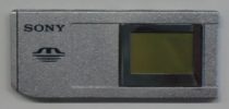
Sony
- (2003 Feb) sensor in the FIU 900: 128x128 @317dpi
- Later, Sony used Authentec sensors in their devices (Microvault).
ESIME Culhuacan [Mexico]
Nagoya University
thermal sensors
optical sensors
Seoul University
NTT
- NTT product page (japan)
- (2004 Jun) NTT launches the FingerQuick FQB-10 with the NTT sensor.
- (2005) NTT Innovative Technology Site P229
- (2005 Sep) µFP 128x128 pixels 508dpi, SPI interface.
Sannaedle > Cecrop / Kinetic Sciences (KSI) > 2005 > Cogent
Dortmund univ.
Siemens > Infineon
LG Philips
TesTech >2009> Integrated Biometrics
Integrated Biometrics
- (2014 Feb) Integrated Biometrics proposes IBtap "the only fingerprint sensor film".
- (2015 Jan) Integrated Biometrics introduced its newest offering: the Columbo Desktop FAP PIV 30 Scanner.
500dpi, 500x400 pixels.
- (2017 Oct) Integrated Biometrics introduced the Five-O FAP 50 scanner.
- (2019 Jun) Integrated Biometrics introduced Danno, a FAP 30 scanner.
Fujitsu Microelectronics America
Who?Vision > 2000 > Ethentica (Security First)
Delsy > Dakty
- (2001) Delsy offers Direct-Optical Scanning (DiOS)
- a CCD sensor (512x576 pixels @1200dpi)
- a CMOS sensor (288x384 pixels @500dpi)
based on optic transmission using some fiber optics. - (2004) discontinued. No more website (www.delsy.de / www.delsy.com)
- (2009) Dakty Naos-1 fiber-optic fingerprint sensor (+fake finger detection) [NAOS: Normal Absorption Optical Sensor]
Fidelica Mycrosystems (2006 > Springworks > 2008 > Palios > 2013 > Lenovo)
- Founded June 1999 by Dr. KG Ganapathi.
- (2001) the FIS-3001 is an area fingerprint sensor made on TFT, based on pressure sensing, using some magnetoresistive semiconductor. An ASIC is flip-chip bonded to the substrate, so that the substrate need not contain any active electronic elements.
Datasheet 2001. Datasheet 2002. White paper.
Some images on Bromba's website.
- (2004 Feb) Fidelica announces the availability of the FIS-3002. TFT substrate from Sanyo.
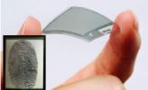
- (2006 Jun) Fidelica moves from TFT to a flexible substrate with a 256x256pixels, 508dpi pressure sensor.
Note the flip-chip silicon chip connected to the array. 1 bit per pixel. - (2006) A smart card is using the Fidelica sensor.
- (2008) Palios buys Fidelica.
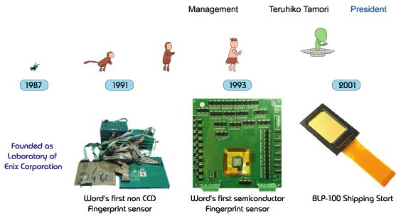
BMF
- (2002 May) Sanyo Electric and BMF (Kawasaki, Japan), subsidiary of Enix, game developer, have formed an alliance to develop products using BMF's pressure-sensitive fingerprint sensor technology using the Sanyo Semicon Device low-temperature polysilicon TFT substrate know-how.
- (2002) BMF BLP-100 datasheet
256×384 pixels @438dpi
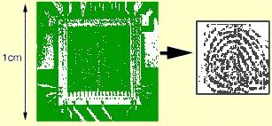
+ Hitachi
- (2003) BMF & Hitachi High-Technologies also proposed the BLP-60, a smaller version, same technology.
168×174 pixels @508dpi / the image is likely the BLP-100...
Kaist & Samsung
NEC
I-Control > 2004 > Atrua > 2009 > Authentec > 2012 > Apple
- (2005 Mar) Atrua Announces World's Most Advanced Intelligent Touch Controls™: the ATw150, ATW210, ATW212.
192x8 pixels @363dpi
- (2009 Jul) Authentec buys Atrua $4.9M. Foundry: UMC.
Tima
Melfas
LighTuning > 2008 > Egistec
- (2003) LTT C500 (A / B with ADC, USB) 236x192 pixels @500dpi
- (2004 Oct) LTT S500: 200x16 pixels @500dpi
- (2006 Jan) LTT SS500: 192x16 pixels @500dpi
- (2008 Mar) LTT SS501 : 192x8 pixels @500dpi. Manufactured by Liteon.
- (2008 Jul) LighTuning is now EgisTec
- SS801U: 192x8 pixels @500dpi.
- (2008) EgisTec SS901: 168x4 pixels @500dpi.
- (2009 Dec) EgisTec ES603-AF (All-Flat Design, black coating): 192x4 pixels @500dpi.
- The ES603-WB is also released.
- (2014 Feb) EgisTec ES608 (swipe).
- (2015 Jan) EgisTec announces the EH570, the world’s smallest rectangle shaped fingerprint touch sensor in EgisTec’s lineup.
23.02 mm2 - Video Egistec at CES2015
- (2016 Jun) EgisTec announces the ET320, integrated in the Samsung C7, A5.
- (2016 Nov) EgisTec announces the ET510, integrated in the Samsung On5 & On7. 100x52 pixels
- (2016 Nov) Egistec partners with Suprema (BioSign algorithm).
- (2017 Feb) Egis Technology will be debuting its brand new under glass fingerprint sensor that can be used with a cover glass of over 1000um at MWC.
- (2020 Jan) Taiwan-based Egis Technology (EgisTec) and eMemory Technology have gained government subsidies for their joint development of large-area in-display optical fingerprint sensor chips.
Hitachi
Mitsubishi
Digital Persona > 2014 > CrossMatch > 2018 > HID
- (2018 Jun) Nomad 30 datasheet (FAP 30)
400x500 pixels @500dpi capacitive TFT / 12 frames/s
TST Biometrics
Ultrascan > 2013 > Qualcomm
- (2007 Sep) Backed by a new $5 million investment from L-1 Identity Solutions, Ultra-Scan is working to develop and make a new fingerprint reader that is much smaller than current scanners and is able to scan four fingers, instead of just one.
- (2013 Mar) Qualcomm acquires Ultrascan.
- Ultrascan has developped an ultrasound TFT device, 4 fingers as announced in 2007.
- (2015 Mar) Qualcomm announces the launch of Qualcomm® Snapdragon Sense™ ID 3D Fingerprint Technology.
- It seems there are two demos at the MWC2015: a regular sensor, and the same(?) below a glass, to demonstrate the ability of capturing fingerprint through the display glass. In the last case, the image is becoming very noisy (this is maybe the reason why there is the logos on screen?). 3D image, they said... check out Vkansee to compare. It seems that dry fingers are still a problem...
- (2015 Jun) Xiaomi is said to be introducing a fingerprint scanner named Sense ID with the Mi 5.
- (2015 Dec) The LeTV (LeEco) LeMax Pro is announced with the Sense ID sensor.
- (2016 Jan) LeMax Pro unveiled at the CES. Sensor seems to have a very different shape. And it is not below the display... Is there some problem with the glass thickness?
- (2016 Aug) reverse engineering from Yole 400 microns metal thickness,
14400 pixels (192x75? 200x72?) @508dpi, LTPS + PVDF (as described in patent). - (2016 Sep) First time underglass (with a recess) in the Xiaomi Mi 5S.
- (2016 Apr) Sense ID O6001 Identification Flats livescan device at 500 ppi (FBI certified product).
4-finger 3.2"x3", TFT ultrasonic image capture. M6001: mobile version.
- (2018 Jul) A Qualcomm under display sensor is announced in the Huawei Honor 10 and the Samsung Galaxy S10. A comeback?
- (2018 Dec 4) Katouzian announced Qualcomm® 3D Sonic Sensor, the world’s first commercial ultrasonic fingerprint solution supported under the display
- (2019 Feb) The Samsung Galaxy S10 is the first commercial device to support the latest Qualcomm® 3D Sonic Sensor. Reads the 3D contours of your physical thumbprint – not a 2D image of it – for improved anti-spoofing.
- (2019 Mar) iFixit Galaxy S10 teardown.
- (2019 Mar) TechInsights Galaxy S10 teardown. QBT2000 ASIC on the flex substrate. 4mm x 9mm sensor.
- (2019 May) General Interface Solution (GIS) is currently producing in-display fingerprint sensor modules at a rate of 2-2.5 million units a month.
O-film is also producing the product.
- (2019 Sep) Samsung to adopt bigger AAD (Active Area Dimension) for Galaxy S11.
The biggest fingerprint AAD that GIS is capable of mass-producing measures 64 square millimeters (8x8mm). The company revealed a 600 square millimeter at Touch Taiwan 2019 last month, but GIS says the product is a work in progress.
- (2019 Dec) The 20x30mm sensor is unveiled. Announces 1 to 1 million FAR (like Apple for its FaceID), which could make sense when you acquire two fingers: the larger the sensing area, the better. Called "3D Sonic Max".
- About the Galaxy S10 disaster when using a cover:
"It's practically impossible to try to predict what types of patterns will be available or what types of covers," Katouzian said. "We are constantly buying different covers and different materials to make sure the algorithm can tell the difference between a legitimate fingerprint and a spoof."
- (2021 Jan) Introducing Qualcomm 3D Sonic Sensor Gen 2
Qualcomm 3D Sonic Sensor Gen 1 was 4x9mm (surface area 36mm2). Gen 2 will debut with a sensor that is 8x8 (64mm2). - (2021 Jan) The sensor is released inside the Galaxy S21. Thank you JerryRigEverything for the teardown.
This is not the very large 20x30mm sensor: likely too expensive.
GIS General Interface Solution
Seiko Epson
Yonsei University (Korea)
Hanshin University (Osan, Korea)
Aqua Buche
Validity > 2013 > Synaptics
- (2007 Jan) VFS201 (USB) and VFS202 (SPI) using Dual Line Imaging is announced.
- (2008 May) VFS201 modules.
- (2009 Jul) VFS301 modules are shipped to notebook PC OEMs.
- (2009 Aug) Customizable LED fingerprint sensor
- (2010 Jun) The VFS5111 fingerprint sensor provides tri-color LED support and enhanced performance...
- (2012 Jun) VFS495: encryption, match-on-chip...
- (2010 Jun) VFS5131
- (2010 Jun) VFS5302
- (2012 Jun) VFS6101
- (2012 Jun) VFS6102
- (2013 Oct) Synaptics buys Validity.
- (2014 Apr): Chipworks tears down the Galaxy S5: confirms this is a Synaptics/Validity chip inside.
- It seems that the metallic border of the button is used as a ground or signal line, likely useful for the sensor itself.
- So there is the Validity chip on a flex -as usual-, but this time there are balls to go to the upper part of the button: it is likely that the conductive lines are directly done on the inside part of the button. I wonder about the number of "pixels", because the number of balls is pretty low, so likely a not so good resolution...
- Let's call this chip the VAL004A8 :) Take care of the die mark, dated 2008, which is confusing...
- (2015 Mar): Synaptics announces the expansion of its Natural ID™ family of solutions with mass production of its small area touch sensor for secure fingerprint authentication in smartphones, tablets, and notebook PCs.
The minimum touch area measures 4 mm by 10 mm. - Year (2013) on the photo is surprising. Likely an old photo.
- The Natural ID family as shown at MWC2015: FS4300, VFS6100, VFS7500.
- Synaptics is proposing "Match-on-sensor" (via Planet Biometrics) which is a solution close to Smart cards.
- (2015 Sep): The Vibe P1 contains the Synaptics' Natural ID area touch fingerprint sensor FS4202.
- (2015 Nov): annouces a live demonstration at the CES of their Natural ID fingerprint authentication technology under greater than 200µm cover glass. Let's bet that we'll see no image at all, only the match/no match. And no FAR/FRR numbers.
- (2016 Jan) Synaptics introduces the name "Ironveil". Prototype in a mouse.
IronVeil product brief. 10x4 mm imaging area.
- at the MWC:
- (2016 Feb) Synaptics Introduces Ultra Slim Area Touch Fingerprint Sensor: the FS4304. 3.5mm wide.
- (2016 Feb) Synaptics Adds Proprietary Anti-Spoofing to SentryPoint Security Suite: proprietary anti-spoofing algorithms.
- (2016 Mar) The Samsung S7 has the BI202A chip dated 2014 (Sitri)
- (2016 Aug) Synaptics Sampling Third Generation Natural ID Under-Glass Fingerprint Sensors: FS4500
- (2016 Aug) FIDO Certified Synaptics Products:
- VFS7500S (Match-in-Sensor)
- VFS7500 (Match-on-Host)
- FS4200 (Match-on-Host)
- VFS6100 (Match-on-Host)
- (2017 Mar) Synaptics announces the FS4600 Fingerprint Sensor Family.
The versatile FS4600 family supports square, round, pill shape, and slim rectangular buttons for the front, back or side of devices. The buttons enable OEM choice of coatings including polymers, ceramics or glass. Value-added features include support for two 0D soft buttons, force sensing and swipe navigation. Sample in CY17Q2 with mass production in CY17Q3.
- (2018 Jan) Vivo X20 Plus is the first smartphone with a hidden fingerprint sensor.
- (2018 Feb) Tear-off from JerryRigEverything.
Note the unusual angled position of the sensor.
Alps Electric
Casio + Alps Electric
Casio
- (2004 Oct): Casio shows at the CEATEC a phone prototype with a transparent TFT sensor directly put over the display.
368×368 pixels @420dpi
Demonstration movie (.wmv)
- (2008) Casio fingerprint sensor using HAST (Hyper Amorphous Silicon Technology).
256x300 pixels @ 508 dpi. Installable on display. COF50M0401ALX - (2008) the LS192 is incorporated in a SDKK device.
CrossMatch >> Sonavation
- Sonavation is a spin-off from Cross-Match launched in July 2006. Technology is called surface impedance impediography, an ultrasonic sensor.
- (2009 Mar) Sonavation unveils the SonicSlide STS3000.
- (2017 Jun) The STS3000 BGA is still available in China!
- (2013 May) a new sensor is unveiled : STS3050.
- (2013 May) ISO 7816 smart card announced (Biocryption) with the sensor.
- (2015 Jul) Announced as "underglass" with a Gorilla Glass from Corning. Likely to say like Qualcomm...
- (2015 Nov) A new brand name: SonicTouch™, and sensors: T4900 (4x9mm, underglass) & T6600 (6x6mm bare+protective coating)
- (2016 Feb) Sonavation Announces Fingerprint Imaging Through Smart Phone OLED Display
- (2016 Nov): leaks about the Meizu Pro 7 with a Sonavation sensor!
Symwave > 2010 > SMSC > 2012 > Microchip
Mitsumi
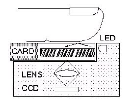
- (2004 May) Mitsumi demonstrates an optical sweep fingerprint sensor.
EDN: the fingerprint sensor has a built-in linear image sensor and light-source LED in a resin-packaged unit. - (2005 Jun) Mitsumi (japan) announces an optical sweep fingerprint sensor, the SEF-A1F1:
256x1 pixel @600dpi.
Flyer 2005.
Flyer 2008 (flex). - (2006) SEF-A1F2 or SEF-A2? faster and reduced power consumption.
- Likely processed by Denken semiconductors.
ElecVision > 2006 > Mediatek
- (2005) ElecVision released the EVS060A an optical sweep fingerprint sensor. The fingerprint sensor has a built-in linear image sensor and light-source LED in a resin-packaged unit.
It is used in the EVM620M module and Trilobyte Tech MB8108-EVS060 module.
256x30 pixels @500dpi - Elecvision is acquired by Mediatek end of 2006. See also Goodix.
NanoIdent
Silicon Display Technology
- (2005 Oct) Silicon Display Technology (Korea) unveils a serie of TFT fingerprint sensors:
SD0250N, SD0360N, SD0360FP, SD0360FA, SD0500N (=SDF500C ?) - (2009) Developped a flexible TFT fingerprint sensor (no info)
- (2013) GOS-1 glass optical sensor, LTPS TFT array 256x360 508dpi.
also announced: GOS5 750 X 800 pixels, GOS4 400 X 500 pixels, GOS3 256 X 360 pixels
- (2013) GCS-2 glass capacitive sensor, LTPS TFT array 256x360 508dpi
Polytechnique Montréal
LiteOn Semiconductor
- (2006) Lite-On releases the FLB6100 (local copy).
Also distributed by [bellus.com.tw/fingerprint.html] Bellus under FX1 name.
616 pixels @1200dpi or 308 pixels @600dpi. - (2006 Jul) There is also an announcement about the FLB8100 (wireless handsets) & FLB8200 (notebooks) [http://mobiledevdesign.com/news/optical-fingerprint-sensor-provide-unique-identity-wireless-handsets].
National Tsinghua university
- (2020 Mar) A 368 × 184 Optical Under-Display Fingerprint Sensor With Global Shutter and High-Dynamic-Range Operation / Chih-Wen Lu et al. / presented at the CICC.
368×184 pixels @1154dpi, optical under-display fingerprint sensor. 120 dB dynamic range. 9.74mm × 4.6mm chip size, 73% sensing area.
Sharp
Imtek
- (2007 Mar) Imtek and Cross-Match are developping a foil sensor based on passive impedance.
AU Optronics
- (2019 May) AUO to Unveil World’s First(*) Full Screen Optical In-cell Fingerprint LTPS LCD Technology
AUO’s 6-inch full screen optical in-cell fingerprint LTPS LCD is the first of its kind to have installed an optical sensor within the LCD structure. Equipped with AHVA technology, full HD+ (1080 x 2160) resolution and 403 PPI pixel density, the panel has a full screen sensing area with the same 403 PPI sensor density and 30 ms swift sensor response time for the smoothest and most accurate sensing performance possible on a smartphone. / Cooperation with Egis
- (2020 Apr) AUO leads to debut TFT optical fingerprint sensor with world’s highest pixel density, and the largest ultra-thin LTPS TFT fingerprint sensor module
AUO will present the unique ultra-thin LTPS TFT optical fingerprint sensing module, with a sensing area of up to 2.9-inch, integrated under OLED panel and a 6.4-inch LCD panel incorporating finger recognition, touch and display functions Offers a large customized sensing area of up to 50mm x 50mm. Besides the application of in-cell touch technology and a three-in-one integrated IC, the 6.4-inch LCD panel breaks through the limits when integrating CMOS image sensor structure to existing panels to offer a large customized sensing area of up to 50mm x 50mm. [...] AUO will also demonstrate a TFT optical fingerprint sensor with the world’s highest pixel density(*) up to 1000ppi, which can [...] also detect the heartbeat.
New Imaging Technologies (NIT)
National Chi Nan University
E-Smart Technologies
- (2003) Super Smart Card
- (2009 Mar) E-Smart unveils a flexible fingerprint sensor manufactured by BMF.
The developed fingerprint sensor consists of a sheet of pressure-sensitive material on top of a thin-film transistor (TFT) made of amorphous or poly-crystalline silicon, with a thin stainless steel substrate (with University in Korea) (video on YouTube).
Institute of Microengineering and Nanoelectronics (IMEN)
FlashScan3D
GelSight
ASD
Morix
- (2017 Nov) Morix FPSF 105 AU
160x160 pixels @500dpi (likely another avatar of the SF105, see below).
OST Oriental System Technology (Orisystech)
Startek & IMD Image Match Design 映智科技股份有限公司
- (2014) IMD SF201: 208x288 pixels @508dpi = FP200
- (2015) The Biosec TS-1011 was 208x288 pixels @500dpi =SF201? (source)
- (2017) now called SF2 Serial (medium size)
- (2014) IMD SF301: 256x360 pixels @508dpi = Startek SFC360 or FP300
(note: same size as the legacy Upek sensors) - (2017) now called SF3 Serial (large size)
- (2015) IMD SF105: 160x160 pixels @508dpi. Likely the same chip for Biosec.
- (2016) The Startek SC160 is a 160x160 pixels sensor. Likely the same. And likely done by Elan eFSA160S
- (2017) now called All in One chip (small size): combo FP+MCU+algorithm [IMD] and FSC160 [Startek]
- (2020) seen at Micropixel Optronics: iMD SF1253P
Biosec 贝尔赛克
- (2015) Biosec TS1012 is a 176x176 pixels sensor. The same as Elan?
- (2015) TS1013M : 176x176pixels @508dpi. Datasheet.
- (2015 Aug) TS1090: 120x120 pixels sensor @508dpi. White,Black,Gold. Datasheet.
- (2015 Oct) TS1060: 176x176 pixels sensor @508dpi. Datasheet.
- (2015 Oct) TS1070: 176x176 pixels sensor @508dpi. Datasheet.
- (2015 Oct) TS1071: 176x176 pixels sensor @508dpi. Datasheet.
- (2015 Oct) TS1071M: 176x176 pixels sensor @508dpi. Datasheet.
- (2016) TS2010M: likely another variant.
- (2016) TS2066M: likely another variant "small area". (M : module version)
- (2016 Oct) TS2022: "large area".
- (2016 Oct) TS2588: "small area".
ADH-Technology
JP Sensor 金鵬微控科技有限公司 >> IFE
- (2010) JP Sensor (a Super Wings subsidiary) releases its first fingerprint sensor, pressure based, the JP1000. 256x256 pixels @ 500 dpi
- Proposed by Fingerprint-tec / ShenZhen WenKe
- (2014) JPSensor proposes smart card application.
- (2015 Sep) Precise Biometrics has entered an agreement with JP Sensor for licensing of Precise Biometrics’ products for fingerprint recognition, Precise BioMatch™ Embedded and Precise BioMatch™ Mobile.
- (2014) The JP2000 is capacitive, 192x192 pixels @ 508dpi.
- (2015) The JP2050(S) is likely using the same chip, different package.
- (2014) The JP2210 is likely the JP2000 (192x192 pixels @508dpi), with another package.
- (2015) The JP2250 is likely just an update.
- (2015) The JP2650 is another package.
IFE Infinity Electronic Biotech
- (2016) JP Sensor becomes IFE Infinity Electronic Biotech. Products are renamed.
- IFE305 capacitance sensor (192x192 pixels @508dpi)
- IFE338 module (same sensor)
- JP2250 -> IFE336 (same sensor)
- JP2650 -> IFE365 (same sensor)
Aculab (Univeristà degli Studi Roma Tre)
Picofield > 2013 > Idex
- (2011) Picofield is developping a new sensor, using a technology more or less derived from Validity (the R&D responsible was formerly Validity) but not swipe-based. It looks like a regular capacitive touchpad, but with a higher resolution (images from patents).
- (2013) Idex is set to acquire the assets and intellectual property rights from PicoField Technologies.
Chalmers University of Technology
UC Berkeley Swarm lab >> Invensense >> 2017 >> TDK
Finchos 成都方程式电子有限公司
- (2015) FSC1001b: 8x128 pixels @ 508 dpi. FSC1001b datasheet.
It looks like the Atrua ATW310. - (2015) the JinMei Tech JM8001 is based on the FSC1001b, with a different package.
Next Biometrics
- (2013 Dec) Next Biometrics becomes public and unveils a new active thermal sensor, composed of an area sensor (LTPS -Low Temperature Poly Silicon- Thin Film Transistors and Devices) on + a silicon companion chip to drive and read the sensor.
All proposed products are using the same TFT sensor, 180x256 pixels @385dpi, 11.9 mm*16.9 mm, in PCB or FPC:
- NB-1010-S : SPI interface, NB-1010-U : USB interface, NB-2010-S : customizable
- (2015 Feb) NB-2020-S (serial interface) (flyer 2015 Nov) (flyer 2016 Dec)
- (2016 Dec) NB-2020-U = NB-2020 USB interface (flyer 2016 Dec).
- (2015 Feb) NB-1011-S (serial interface)
- (2015 Oct) Next will deliver 1.2 million sensors to Dell in 2016.
- (2016 Feb) NB-1411-S embedded module (flyer)
- (2017 Jun) Innolux shows the flexible sensor developped with Next Biometrics.
- (2019 Jun) One Touch Access CT-150 flexible module for smart cards (flyer 2019 Jun).
180x256 pixels @385dpi
- (2019 Jun) One Touch Flex CT-150 (flyer 2019 Sep) / 180x256 pixels @385dpi
- (2019 Sep) One Touch Access 100-USB Module (flyer 2019 Sep) / 180x256 pixels @385dpi
- (2019 Sep) One Touch Access 100-SPI Module (flyer 2019 Sep) / 180x256 pixels @385dpi
- (2019 Sep) One Touch Access 110-SPI Module (flyer 2019 Sep) / 180x256 pixels @385dpi
- (2019 Sep) One Touch Access 115-SPI Module (flyer 2019 Sep) / 180x256 pixels @385dpi / extended temperature range -30°C,+60°C
- (2019 Dec) One Touch Access 200-SPI Module (flyer 2019 Sep) / 180x180 pixels @385dpi
- (2019 Dec) NEXT One Touch ID is PIV certified (FAP20): Model NB-65210-S single finger livescan capture device at 500 ppi.
500 dpi? but it's a 385dpi sensor? Ah! "optical equivalent resolution" : very clever.
Shenzhen Betterlife Electronic Science and Technology
深圳贝特莱电子科技股份有限公司
- (2015 Jul) BL2380 8x160 pixels @ 508dpi
BeyondEyes
- (2013) BeyondEyes is developing near infra red based world's thinnest (1mm) and high resolution (2500dpi) optical fingerprint recognition sensor for mobile device as the personal authentification purpose.
SunASIC
- (2013) SunASIC is a company providing services about fingerprint sensors: design & wafers.
- (2013) Delivered a first generation fingerprint image sensor.
- (2014) Delivered a second generation fingerprint image sensor.
- (2016) Delivered a third generation fingerprint image sensor.
- (2018) The A365 sensors received FBI PIV certification, and the company has been granted 20 US patents.
- As of 2022 Feb:
Customers:
- JPsensor (2013~, first fingerprint sensor)
- Biosec Co. Shanghai (2015~)
- Zteway Co. Beijing (2015~)
- Suprema Inc. and other Korean customers (2018~)
Partners:
- Avision Inc., Taiwan
- BIOSEC Technology Co., Ltd., Shanghai
- Nuvoton Technology Corporation
- STMicroelectronics N.V.
- Suprema Inc.
- Zteway Technology Co., Ltd - Company description (Feb 2022)
- Product lines (@500dpi): (you will also find the products under the ByNew brand)
- 112x88 pixels
- 120x120 pixels
- 160x160 pixels
- 176x176 pixels
- 192x192 pixels
- 208x288 pixels : A-285-MRC (datasheet rev 003) A-285-MRC (user manual rev 001) (see also ByNew)
- 256x360 pixels
Holtek
- (2016 Jul) A new reference appears: GH-8511, under development, available in 1Q, 2017.
320x320 pixels @1000dpi. Ultra-thin package with Heart Beat Monitor & Wake-up on Fingerprint.
MicroArray Co. Ltd. 苏州迈瑞微电子有限公司
- MicroArray is developping active capacitive fingerprint sensors, using a patented variant called CQT by MicroArray.
- (2014 Mar) AFS192 192x256 pixels @504dpi (50.4μm) SPI 60 fps @24MHz
- (2014 Sep) AFS120T, 120x120 pixels @508dpi, TSV packaged, ZrO2 ceramics covered module for smart phone market. datasheet v1.31
- Microarray TSV packaged its fingerprint sensor with Speed Semiconductor one year before Apple with its iPhone6S's Touch ID, instead of trench + wire bonding package.
- (2014) Microarray supported Sanhuan developing ZrO2 ceramics as cover plate for fingerprint module. FPC used this material in Xiaomi Mi5 in 2016.
- (2014 Sep) 200 microns of Zircone (Apple: 260 microns of sapphire) give less degradation to the image, but still requires some specific enhancements.
- As the AFS120 is small, pattern matching is used.
- (2015 May) AFS120M, 120x120 pixels @508dpi, molding + coating packaged single chip solution, with bezel. datasheet v1.0
- (2014-2015) Microarray help Sumitomo developing high DK molding compound for fingerprint sensors. Since 2015, this version of Sumitomo’s compound is widely used.
- (2015 May) AFS080T: 192 x 80 pixels @ 508dpi
- (2015 July) AFS120N, 120x120 pixels @508dpi, molding + coating packaged single chip solution, without bezel. datasheet v1.1
- (2015 July) AFS080U: 192 x 80 pixels @ 508dpi, 300um - 400um glass
- (2015) Upcoming: (touch) AFS160, AFS200, AFS360, (swipe) SFS192.
- (2016 May) The 4th generation Microarray 3D fingerprint sensor is in the UMI Super.
- (2017 May) Roadmap
Goodix
- (2014 May) Goodix formerly known as Shenzhen Huiding Technology Co. Ltd. (a subsidiary of Mediatek, see also Elecvision), introduces a new active capacitance fingerprint sensor. Goodix presentation (OFweek).
By adopting a new original patented packaging technology, Goodix integrated the metal ring, sapphire cover and sensor into a small volume. The mode of operation is similar with Apple Touch ID technology. Products: GF6616, GF6626, GF6610 and GF6620. Minimum size is only 9.76mm x7.4mm x1.17mm.
Announced accuracy: FAR 1/50000 for a FRR 1/100 (at least, they give the FRR: Apple said nothing about that).
- (2014 Sep) Goodix unveils their new generation of fingerprint identification solution - IFS (Invisible Fingerprint Sensor), developped with TPK which should enable to remove the ring, and use directly glass (450 to 700 microns thick).
300 microns sapphire protection (like the Apple 5S).
- (2015 Jun) New names? [with coating: GF316, rear GF318] [with glass: GF516, rear GF518] [GF919, GF816]
- (2016 Feb) Goodix to Unveil Advanced Fingerprint Sensor That Rejects Fakes at MWC 2016: world’s first Live Finger Detection™ technology. Senses the users' pulse to reject spoofs.
BTW, Goodix is using Authentec's drawing explaining their sensing technology, which was already an explanation that it was working with live fingers :) Also, not afraid of patent infringments... Note also the "Samsung" name.
Aliveness detection is not really new. And what if we use a thin fake over a real finger?
- (2016 Oct) Some info about generations of sensors, clarifying the situation.
- (2016 Oct) Packaging & IFS.
- (2017 Feb) Inside the Zuk Edge (U Touch)
- (2017 Feb) ABIresearch teardowns unveils the AC2201TC2 chip from Goodix with an "heart beat" detector. (via Eetimes)
capacitive 128x60 pixels @500dpi (similar to GF52xx devices)
- (2019 Jun) Redmi K20 Pro in-display sensor.
- (2019 Dec) Shenzhen Goodix Technology Co., Ltd. today announced that its ultra-thin optical IN-DISPLAY FINGERPRINT SENSOR™ officially ushers in the 5G era with the commercialization by OnePlus 7T Pro 5G McLaren released in the United States.
- (2020 Apr) Goodix’s Ultra-Thin Optical In-Display Fingerprint in OnePlus 7T Pro 5G McLaren (System Plus reverse engineering). On-chip Near InfraRed (NIR) filter, collimator and MicroLens Array (MLA).
Silead 思立微 > 2018 > GigaDevice
- Silead (subsidiary of GalaxyCore)
- (2014 May) Silead unveils the GSL6162: 508 dpi, 5.5 x 5.7mm sensing area, FRR<1% FAR<0.01%. Possibly O-film for packaging.
- (2014 Nov) Silead is securing fingerprint sensor orders from Coolpad and ZTE.
- (2015 May) Precise Biometrics announced it signed a license agreement with Chinese fingerprint sensor manufacturer Silead to include Precise Biometrics´ fingerprint software, Precise BioMatch Mobile into its products portfolio.
- (2015) GSL6163, GSL6172, GSL6182, GSL6185, GSL6263, GSL6272.
- (2017 May) Oppo is working with Silead about the brands's GSL625x sensor.
6.8x2.4mm @508dpi
- (2019 Mar) GigaDevice bought Silead in January 2018 for 1.7 billion yuan, approved in March 2019.
- (2020 Apr) Product Selection Guide
- Capacitive fingerprint sensors (sensing area, pixels)
- GSL6157N 8.0 x 1.8 mm 160 x 36
- GSL6257N 8.0 x 1.8 mm 160 x 36
- GSL6150N 4.0 x 3.2 mm 80 x 64
- GSL6250N 4.0 x 3.2 mm 80 x 64
- GSL6185E 5.7 x 6.6 mm 114 x 132
- GSL6156E 6.8 x 2.4 mm 192 x 68
- GSL6182E 8.0 x 8.0 mm 160 x 160
- GSL6275E 8.8 x 3.2 mm 176 x 64
- Optical Fingerprint Under OLED (FRR<.5%@FAR<1/50,000) (sensing area, pixels)
- GSL7000A 6.0 x 6.0 mm 320 x 320
- GSL7001A 6.0 x 6.0 mm 320 x 320
- GSL7001F 6.0 x 6.0 mm 320 x 320
- GSL7301A 6.0 x 6.0 mm 88 x 86
- GSL7303A 6.0 x 9.0 mm 180 x 280
- GSL7305A 6.0 x 6.0 mm 180 x 180
- GSL7253 30 x 20 mm 300 x 200
- Ultrasonic FP Under OLED (sensing area, pixels)
- GSL8165A 4.8 x 4.8 mm 80 x 80
- GSL8252 30 x 20 mm 428 x 285
J-Metrics / Jinhuaxin
- (2017 Mar) Taiwan J-Metrics (Shenzhen) and PEKING University signed an alliance with MEMS based ultrasonic fingerprint sensor.
FocalTech 敦泰電子股份有限公司
- (2016) FT9306: 64x160 pixels @ 508dpi.
- (2016) FT9308/9338/9538: 88x 88 pixels @ 508dpi.
- (2016) FT9336/9536: 64x128 pixels @ 508dpi.
Elan
- (2014 Aug) Elan Microelectonics is developping fingerprint sensors optical type and capacitive type, with Startek.
- (2014 Aug) Startek Engineering and Elan are making a strategic alliance.
- (2015 Mar) a 176x176 pixels sensor, 8.8x8.8mm and a 120x120 pixels, 6.4x6.4mm are developped.
- (2015 Oct) The Startek SFC176 is a 176x176 pixels @508dpi fingerprint sensor.
- (2015) Biosec TS1012 is a 176x176 pixels sensor. The same, different coating?
- (2016) The Elan eFSA160S is also likely the Startek SC160. 160x160 pixels @500dpi
- (2017 Apr) Taiwan-based Elan Microelectronics has announced it is teaming up with smart card integrator Jinco Universal and Korea Smart ID (KSID), a security solution provider, to develop smart cards with an embedded fingerprint sensor.
- (2018 Mar) Some sensors showed at MWC2018: eFSA614RA, eFSA96SA, eFSA80SA, eFSA688RA.
- (2021 Aug) Sensors from the Elan website:
eFSA515RT 150x52 pixels @508dpi 2% FRR @ FAR 1/100,000
eFSA80ST 80x80 pixels @508dpi 2% FRR @ FAR 1/100,000
eFSA680RM 80x64 pixels @508dpi 2% FRR @ FAR 1/50,000
eFSA56SM 56x56 pixels @508dpi 3% FRR @ FAR 1/50,000
Vkansee
- (2015 Jan) Vkansee formally released UTFIS, an ultra-thin optical fingerprint sensor, at the CES.
- UTFIS uses advanced pinhole imaging techniques to take a high-resolution image that requires neither a lens system nor a prism for reflecting the light.
2000dpi, 1.5mm thick, size: 11,25 × 7 mm (TBC), 8x12 pinholes
- Announces that a fake finger can spoof an Apple Touch ID sensor (not a big deal), but not their sensor (it would be better to stay humble on that subject...), thanks to the third level features (pores).
- See the sensor working on this video from mobiwatchEN
- See the sensor working on this video from CNET, with a not so contrasted image, likely from a dry finger (bad luck, guys).
- (2016 Feb) Vkansee unveils the VK2108 at the MWC. Smaller: 6 x 3.5 x 1.5 mm @2000dpi. (I know, it's written FP8801 on the flex).
- (2016 Feb) Vkansee is demonstrating an attack using fake fingers at the MWC: techradar, htxt.
Aliveness detection is not really new.
Trais 트레이스
BYD Build Your Dreams 比亚迪股份有限公司
- (2015 May) BYD Build your dreams made a conference in Shenzhen. Two front fingerprint chips + a rear fingerprint chip were presented:
- BF6611A : front, 508 dpi, 144x72 pixels wafer-level packaging + cover, 3.7x8.7mm chip size
- BF6621A : front, 508 dpi, plastic coating module
- BF6631A : rear, 508 dpi, 160x160 pixels, 10.4x10.4mm chip size FRR 0.01, FAR 1/200 000 (!)
90 patents applied. Coating 200um.
Jenetric
- (2015 Sep) Jenetric presents their first sensor Livetouch quattro. A large optical TFT FAP60 sensor, so at least 3.2"x3" @ 500dpi (1600x1500 pixels).
- (2016 Sep) Jenetric presents the Livetouch quattro Compact.
Langevin Institute
Lustrous Electro-Optics
Sunwave 信炜科技
- (2015 Dec) Sunwave (Shenzhen) unveils some info about new capacitive sensors:
SW9580 : under glass 400um / SW9581 600um
SW9560 : over molding <300um
SW9551 : coating (SW9550 is likely a former version)
- (2016 Oct) A new sensor: SW9651 / 9661
- (2016 Dec) main product: SW9562N
Chengdu Finger Technology (CDfinger) 成都费恩格尔微电子技术有限公司 >> FingerTech
- (2015) Chengdu Finger Technology "Ultra-Scan" RF capacitive fingerprint sensors
- FPS? 160x8 pixels @508dpi, FRR 0.01% FAR 0.0001%
- FPS0160 160x160 pixels @508dpi
- (2016 Mar) Roadmap presentation.
- FPS1398
- FPS2198 / FPS1498
- FPS3098 underglass
- FPS3056 underglass
- (2016 Mar) FPS1398 : 96x96 pixels @508dpi
- (2016 Dec) roadmap
- FPS1358 (replaces FPS1398E)
- FPS1356 (replaces FPS1256E)
- FPS958, FPS968 (replaces FPS998E / FPS1198)
- FPS1598 underglass
- (2017) FPS1256E, FPS1356E
- (2017 Apr) Introducing FingerTech brand. 成都费恩格尔微电子技术有限公司
Chipone
- (2015 Oct) Chipone ICNT7183.
ICNT7183: 160x160 pixels @508dpi for placement on the back
- (2016 Jan) some info about the ICNT71xx family.
ICNT7123: 56x192 pixels @508dpi for front / side placement
ICNT7127 & ICNT7187 : advanced versions - (2016 Feb) Precise Biometrics signs license agreement with Chipone.
- (2016 Mar) a new member? with different packages:
ICNT7152, 7153, 7157: 88x112 pixels @508dpi - (2017 Jul) ICNT7236AL LGA 64x150 pixels @ 508dpi / FAR 1/50000, FRR 1%.
Datang Microelectronics Technology (DMT) 大唐微电子
- (2016 Jun) Datang exhibition.
DMT-FS-PB4FS 64x114 pixels @508 dpi (for mobile phones)
DMT-FS-PB4F 208x288 pixels @508 dpi capacitive sensor (=Finchos FSC2002?) (datasheet v1.0)
Also showed the 2nd generation ID card.
Novatek
- Novatek.
- (2014 Oct) Introduced Novatek's first HD CIS ( CMOS Image Sensor ) for fingerprint recognition application.
- (2015 Dec) Introduces first under glass thin type optical fingerprint module.
- (2016 Oct) Introduced Novatek's first front-mount and side-mount fingerprint sensor with Single-Chip and Biometric Live Detection for all cover solutions and high security level.
- (2016 Nov) Introduced Novatek's first back-mount fingerprint sensor with Single-Chip and Biometric Live Detection for all cover solutions and high security level.
- (2017 Sep) Introduced Novatek's first narrow front-mount and side-mount fingerprint sensor with Single-Chip for all cover and 18:9 full screen solutions.
- (2017 Nov) Introduced Novatek's first super thin front-mount fingerprint sensor with Single-Chip for under glass and 18:9 full screen solutions.
- (2020 Nov) Introduced Optical FPR Sensor with Anti-spoofing for under OLED solution.
Super-C Touch
- (2019 Jan) ST-S10GB/C (& SCTFPWS01):
256x360 pixels @ 508dpi, 2 frames/sec, capacitive.
- SuperC Touch’s “Perturbation Resonance” technology
- Off-Chip Capacitance Fingerprint Sensing Technology
Isorg + FlexEnable
- (2016 Jan) FlexEnable and ISORG have introduced a large area flexible fingerprint sensor on plastic. The fingerprint technology is able to measure the fingerprint and also the configuration of veins in the fingers, providing additional security versus that of a surface fingerprint alone.
8.6 cm x 8.6 cm active area, 84µm pitch = 304 dpi, 1024 x 1024 pixel, 0.3 mm thick. Operates in visible and near infra-red up to wavelengths of 900 nm. - (2016 Feb) Demo at the MWC.
- (2016 Oct) FlexEnable & Isorg announces a 500 dpi version.
- Thickness: less than 0.3 mm:
- 1” x 2” : smartcards, mobile phones
- 3” x 3.2” : multi-finger, vein scanners
- (2017 Jun) Image from the Isorg 500 dpi image sensor : fingerprint and vein.
Telecom SudParis
MStar semiconductor
Shanghai OXi Technology 籮箕技術(香港)有限公司
- OXi Technology founded in 2014. (CEO: Hong Zhu)
- (2015 Oct) Lo Kei: A 128x180 optical? fingerprint sensor @508dpi -> likely another name.
- (2015 Dec) Precise Biometrics has entered an agreement with Shanghai OXi Technology.
OXi technology is a biometric sensor company located in Shanghai, Zhangjiang hi-tech park. OXi provides biometric sensors and solutions based on its unique TFT Thin Optical Touch technology. - The technology looks to be a regular TFT sensor over a backlight and below a kind of lens (normal glass? really?), in order to accept a 1mm glass thickness.
- (2016 Apr) first show. M1000 series for consumer market. Sensor is under normal glass (up to 1 mm thick).
128x180 pixels @508dpi
- (2016 Apr) G5000 dual fingerprint scanner.
768x1200 pixels @500ppi (FAP45)
- (2016 Apr) OXi 10-Print Fingerprint Scanner (G4000?)
1536x2400 pixels @500ppi (FAP60)
Shenzhen ChipSailing Technology 芯启航
- (funded 2015 Jul) ChipSailing 芯启航.
- (2016 Aug) Square series: CS1201, CS1501 / CS2511, CS2516, CS2517
- (2016 Aug) Runway series: CS1801, CS1501 / CS2511, CS2516, CS2517, CS2811, CS2816, CS2817
- (2016 Aug) Long strip series: CS1801 / CS2811, CS2816, CS2817
- (2016 Aug) Round series: CS1501 / CS2511, CS2516, CS2517
- CS1501/2511: 112x88 pixels (similar to FPC1022/1035)
- (2017 Feb) CS3716/3711 : 68x118 pixels. Image under 175um glass.
Biolog device
Haptrics 햅트릭스
- (2015) Haptrics 햅트릭스, founded June 2015, is a fabless korean company offering CMOS based fingerprint sensors, highly optimized in terms of performance and cost for smartphone applications.
- (2016 Nov) Haptrics recently released a prototype.
- (2017 Jun) Fingerprint sensor start-up Haptrix expects first sales in 2H. First engineering sample in March. Announced with 635 dpi resolution. Aims also under-display sensors (next generation).
- (2017 Oct) Precise Biometrics enters into agreement with with Haptrics for the licensing of Precise BioMatch™ Mobile. Haptrics plans to release customer samples in November, 2017.
Ulsan National Institute of Science and Technology (UNIST)
PYCSEL project
- (2017 Jan) The Pycsel project is devoted to develop a new fingerprint sensor.
Innovative active thermal sensor, using PVDF-based pyroelectric material, combined with an IGZO TFT matrix foil, capable of high resolution fingerprint capture. - (2019) The Identifying fingerprints by a PYCSEL sensor (CEA website)
- (2019 Mar) The PYCSEL technology was demonstrated at LOPEC 2019 and won the OE-A best Publicly-Funded Project Demonstrator Award. [>> more info <<]
- (August 2019): (press release) PYCSEL, a new thermal fingerprint sensor, winner of the bestPublicly Funded Project Demonstrator Award in the OE-Acompetition, will participate in the EAB conference.
- IEDM 2019 / 65th International Electron Devices Meeting / 10-DEC-2019 / San Francisco
Sensors, MEMS, and Bioelectronics 4:25 PM 26.5 A Large-area Curved Pyroelectric Fingerprint Sensor - SID, Book 1: Session 14: Image Sensors: 14.1: Flexible Large-Area Multi-Fingerprint Sensors Based on Thermal Mass Detection/ Florian De Roose, Jean-François Mainguet et al. (first publication 25 September 2020).
Cornell University + Intel / Geegah / A*STAR
BEFS
Fraunhofer FEP
- (2017 May) The Fraunhofer FEP developed a new generation of its bi-directional OLED microdisplays, that employ an extra-thin encapsulation layer, which can turn these new displays into fingerprint sensors. Native resolution 1600 dpi
CMOS Sensor inc.
- (2017 May) CMOS Sensor releases the C608, an optical fingerprint sensor. With the capability of scanning through thick glass including 2.5D cover glass, C608 offers a perfect solution to eliminating glass cut-out or thinning which are required by contemporary capacitive fingerprint sensor.
- C608 datasheet: 160x240 pixels @1016dpi
Shanghai Jiao Tong University
Sungkyunkwan University SKKU
OT-Morpho >> 2017 >> Idemia
- (2017 Sep) OT-Morpho unveils MorphoTop Slim. Optical TFT / Appendix F.
Senvis
- Senvis (Korea, spinoff from Hanshin university).
- (2017 Oct) Senvis unveils a bezel-less fingerprint sensor at the Sedex.
- (2018 Jul) The SVF10P has 96x96 pixels @508dpi. TSMC 0.25um CMOS. Max coating: 150um. Etnews.
Zeitec / Socle (Foxconn)
Japan Display Inc. (JDI)
- (2020 Sep) Full screen fingerprint sensor, capacitive, 313dpi : Nikkei (YouTube).
Tokyo III SiSOC + DDS
Samsung
- (2022 Jan) Samsung Introduces Smart All-in-One Fingerprint Security IC for Biometric Payment Cards The new security IC solution combines a fingerprint sensor, Secure Element and Secure Processor in one chip, with enhanced security features enabled by Samsung’s proprietary fingerprint authentication algorithm and anti-spoofing technology. (YouTube).
Optimized for the contactless era, 512k flash, 48k rom, 18.5k ram, ISO7816, ISO14443A, 3DES/AES/RSA/ECC Samsung biometric card / S3B512C
It's a surprise that the S3B512C was a integrated one chip solution, because it is costly to use an expensive CMOS process with security features to make a large area fingerprint sensor (no info about size and resolution). See System on chip.
BOE
- (2018 Jul) BOE under-display TFT Fingerprint: BOE shows their new under-display fingerprint sensor at SID Display Week 2018.
960x512 pixels @500dpi TFT under an OLED display.
- (2018 Jul) Organic-Inorganic Hybrid Thin-film Photo-detector for Fingerprint Recognition: A near-IR based optical type fingerprint sensor is designed and implemented. The driving system is based on the passive pixel sensor (PPS) array with Oxide (IGZO) TFT technology. The sensing element of the optical sensor is composed of the organic photosensitive diode (OPD) exhibited typical sandwich structure. (with help from Isorg)
960x512 pixels @500dpi optical OPD TFT near IR
Imec & TNO
- (2021 Nov) A thin and flexible scanner for fingerprints and documents based on metal halide perovskites (Nature Electronics) / Albert J. J. M. van Breemen & als / TNO at Holst centre.
“Because our imager is very thin, it can be wrapped around round objects. This is for instance advantageous in high-resolution, nail-to-nail biometric fingerprint scanning. Furthermore, we show that it can detect your heartbeat simultaneously, which is another safety feature. We believe that our perovskite image sensors are ideal for integration into everyday objects such as the backside of mobile phones and door handles as part of unobtrusive, secure-access control systems,” says Albert van Breemen, senior researcher TNO at Holst Centre, who led the research.
Hi Albert :) it looks you reused the same interface than PYCSEL !
SilTerra
Chungbuk National University CBNU
Sun Yat-sen University 中山大学
- (2018) Highly Sensitive a-Si:H PIN Photodiode Gated LTPS TFT for Optical In-Display Fingerprint Identification /Xianda Zhou, Meng Zhang, Yitong Xu, Wei Zhou, Kai Wang, Arokia Nathan, Man Wong, Hoi Sing Kwok, Hai Ou, Jun Chen, Shaozhi Deng, and Ningsheng Xu.
150x150um2: 166dpi
Chongqing HKC Optoelectronics Technology
BIT Beijing Institute of Technology 北京理工大学
Cypress
Keycore Technology Corp (KCT)
- Keycore Technology Corp (KCT)
- (2018 Oct) Fingerprint drive IC Keycore Technology Corp develops a new generation driver IC for fingerprint authentication. The sensor array uses the glass or non-silicon wafer. The sensor is underneath a flat glass, and is using the driver IC (chip on glass) to read the signal.
Tohoku University
(Xiamen) Tianma Microelectronics 天 马微电
Vivo
- (2019 Mar) Vivo demonstrates the full-screen fingerprint sensor with the Vivo APEX 2019.
Manufacturer? Oxi? Fortsense?
Fortsense
Touch Biometrix
- (2017) Touch Biometrix is founded. Announces " a new type of fingerprint sensor that will disrupt the authentication industry, Revolutionary Fingerprint Sensing Technology". Citing Imec / Holst center / flexible technology, in their Twitter account, BTW.
- (2019 Jan) (via Verdict) The pixel on a [display] screen can be modified so that it can detect capacitance, so when it comes into contact with your finger [the screen] can detect the variation in capacitance between valleys and ridges and curves.
- (2019 Oct) Touch Biometrix Demonstrate First Fingerprint Sensor.
- (2019 Nov) (Touch Biometrics News) [Mike Cowin said:] "this is a great result... and this is an important deliverable on our roadmap to defining and scaling the production of our first minimum viable product in 2020."
- (2023 Jan) The TCAP60 is announced.
- (2023 Nov) The TCAP60 (FAP60 500dpi) is fabricated by Sharp Display Technology Corporation / IGZO TFT based substrate
SEL Semiconductor Energy Laboratory
ByNew Technology
- Bynew Technology Inc. was founded in October/2014 in Taipei, Taiwan.
Partner: SunASIC (manufacturer), ZTEWay (algorithm) - (2020 Feb) Products (sensors) :
- 208x288 pixels @508dpi: A285
- 256x360 pixels @508dpi: A365
NCU National Central University, Taiwan
Midas Touch
- Midas Touch Inc. Taipei, Taiwan.
- Take care: datasheets have errors. Looks to be chips from some other manufacturer.
Documents are dated ~2018: company profile - (2020 Mar) Products (sensors):
- 82x62 pixels @508dpi: MFC-1082
- 160x160 pixels @508dpi: MFC-1160, MFC-1165, MFC-2160
- 192x256 pixels @508dpi: MFC1192
- MFC-1192 (no specific MFC-1192 datasheet)
- 208x288 pixels @508dpi: MFC1201,MFC1208
(TouchChip ? Finchos ? Datang ? ByNew ? IMD ? Biosec ? Betterlife ?)
- 256x360 pixels @508dpi: MFC1256 (C: steel coat)
- 1600*1000 pixels @500dpi: MFC-1600 FAP 50
3M
- 3M NITS.
- (2020 May) 3M introduces new LCD screen optical fingerprint recognition technology called NITS: Near Infrared Transmission System. It takes advantage of the LCD being transparent to near-infrared light. 3M proposes some filters, you need to add a camera.
Technical Data 2020 (local copy)
TCL CSOT China Star Optoelectronics Technology
- TCL CSOT. CSOT owns in Wuhan one 6th generation LTPS (OXIDE) LCD/AMOLED display panel production line and one 6th generation flexible LTPS-AMOLED display panel production line.
- TCL CSOT products fingerprint.
JIIOV
- (2021) JIIOV. New generation of fingerprint technology based on AI.
- History:
- (2019 Nov) Founded
- (2020 Jul) first generation lens type in-display
- (2020 Dec) second generation BSI lens type in-display
- (2021 May) side-key capacitive fingerprint sensor
- List, as of 2021 Nov:
- JV0101 capacitive sensor, side-key, 2.1mm width
- JV0201 ultra-thin in-display fingerprint sensor
- JV0301 lens type in-display fingerprint sensor, BSI technology
- JV0302 lens type in-display fingerprint sensor, BSI technology
- JV0401 chip scale in-display fingerprint sensor
Nanjing University of Aeronautics and Astronautics
Gingytech
to be confirmed...
If you want to get some information about the silicon manufacturers where these silicon sensors are fabricated.